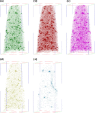
Typical atom maps of P, Cu, Mn, Ni & Si (clockwise from bottom centre) in 65x65x142 nm sample of steel from Styman et al, 2015.
A couple of weeks ago I wrote about the opening plenary talk at the NNL Sci-Tec conference [‘The disrupting benefit of innovation’ on May 23rd, 2018]. One of the innovations discussed at the conference was the applications of atom probe tomography for understanding the mechanisms underpinning material behaviour. Atom probe tomography produces three-dimensional maps of the location and type of individual atoms in a sample of material. It is a destructive technique that uses a high energy pulse to induce field evaporation of ions from the tip of a needle-like sample. A detector senses the position of the ions and their chemical identity is found using a mass spectrometer. Only small samples can be examined, typically of the order of 100nm.
A group led by Jonathan Hyde at NNL have been exploring the use of atom probe tomography to understand the post-irradiation annealing of weld material in reactor pressure vessels and to examine the formation of bubbles of rare gases in fuel cladding which trap hydrogen causing material embrittlement. A set of typical three-dimensional maps of atoms is shown in the thumb-nail from a recent paper by the group (follow the link for the original image).
It is amazing that we can map the location of atoms within a material and we are just beginning to appreciate the potential applications of this capability. As another presenter at the conference said: ‘Big journeys begin with Iittle steps’.
BTW it was rewarding to see one of our alumni from our CPD course [see ‘Leadership is like shepherding’ on May 10th, 2017] presenting this work at the conference.
Source:
